How to trace circuit boards easily

Circuit boards, even small ones, look crazy complicated. But they really aren’t — they’re just efficiently packed. Most circuit boards have just two “layers” of copper traces running around: top and bottom. Something sophisticated like a computer motherboard can have more copper sandwiched in the middle, but most of the things a hobbyist would want to trace are just have a top and bottom.

What can make tracing complicated is that the two sides work together, with a single connection flipping between top and bottom multiple times.  But we can use a camera and an image editor like Paint.NET, Photoshop (the CS2 version is free now), or GIMP to make it easy.

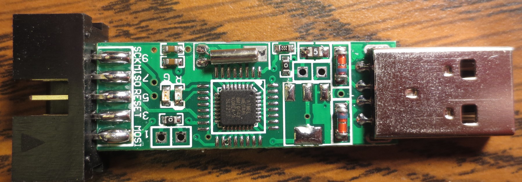
As an example, let’s trace this USB device.  It’s an off-brand programmer for AVR chips that had no documentation and didn’t work in a standard way like similar products, so I had to figure to figure out how it was wired up.

I started by taking good, high-resolution pictures of each side, trying to keep the camera a fixed distance from the board on each side.  Using a document scanner didn’t work for this, because the board didn’t lie flat on the glass…you might be able to use a scanner for a flatter circuit board.

side1side2

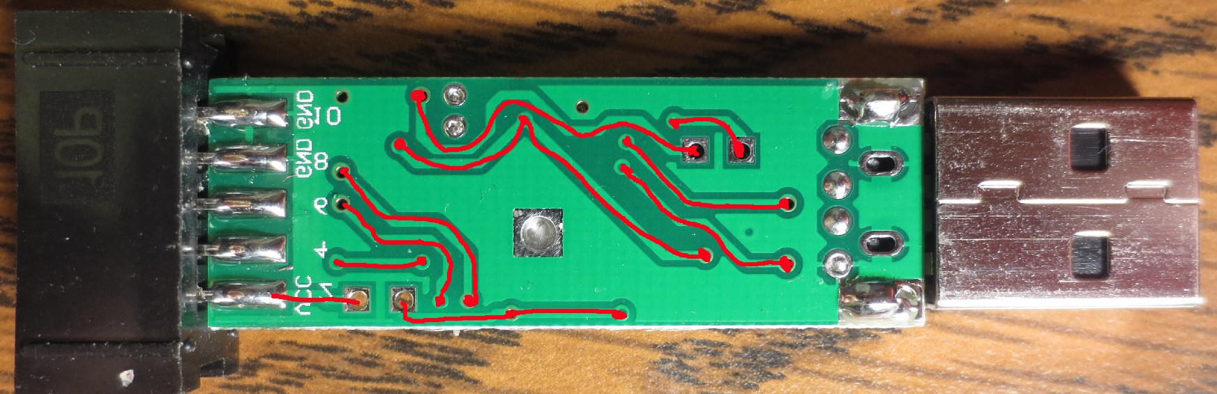
We’re going to superimpose the bottom (simple) side over the top (complex) side in the image editor.  Take the picture of the simple side, copy it, and paste it as a new layer over the complex pic.  Set it to semi-transparent, flip it vertically, then use the layer transform or move tool to get it to line up exactly over the top side of the board.  Be sure to match up key landmarks, like vias (the little holes that connect top and bottom) and through-holes.

Once they match, turn the simple side opacity all the way back up, add a new empty layer, and paint all the traces you see in a high-contrast color (like red, for green boards).  When you’re done, you should be able to slide the opacity of the simple & red layers up and down and have it look like this:

anim2a

Now, turn off the simple layer, but keep the red trace layer.  Now you have a picture of the top of the board with all the bottom-side traces super-imposed:

together

Now you can add another layer and draw additional annotations that you need until you’ve discovered everything you need to know.

together-more

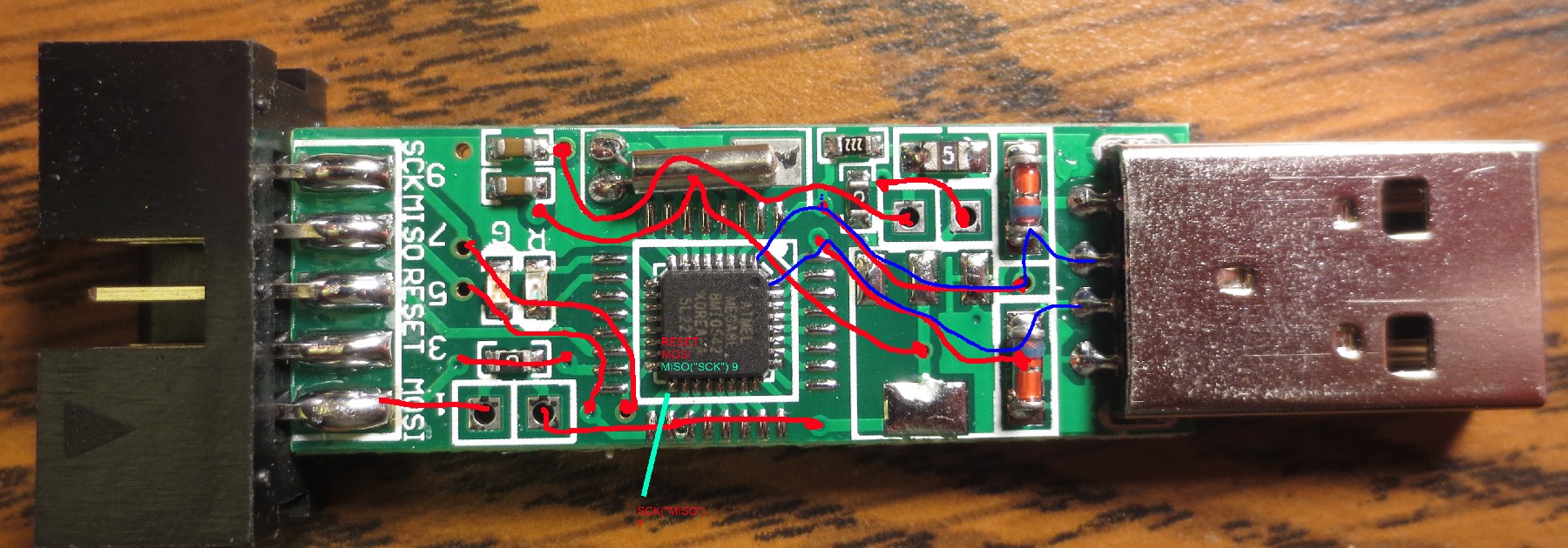
What I needed to know for this board was this: I was dumb to buy this $4 programmer just because it had a fancy case when the well-known good model was nine cents cheaper.  It’s a crappy nonstandard board nobody’s ever heard of, and though I could fix it by adapting custom firmware for it, I’m better off just throwing it in the bin and getting the good one (which I did).

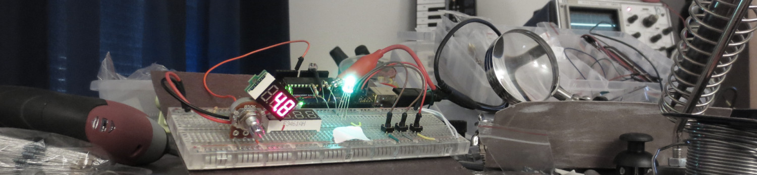
But it was a good exercise in circuit tracing.

Tortilla Pad: A touch pad made out of a tortilla or wet lumber

I’ve been trying to build a touchpad that appears to be different than those I see online.

Normal touchpads, both capacitive and resistive, have multiple layers, so they can be operated with a plain finger or stylus.  This is good, but costs a non-trivial amount of money.

I want to build one with a single layer of simple resistive material (a material with electrical resistance in the 100-100000 ohm range, see here for a list), with a probe connected to an analog voltage sensor (metal pen with a wire on it OR the finger of someone holding said pen).  The advantage would be that you can make ANY resistive material into a touchscreen, regardless of size, just by putting four conductors in the corners hooked up to a microcontroller.

My first prototype was with a fresh tortilla, and I’m very sorry I didn’t get a picture of it.  It looked dumb as hell…I cut a rectangle out of it, hooked alligator clips to the corners, and toggled voltage at the corners with Arduino data pins, reading the voltage of a probe placed on the surface with an analog pin.  It worked okay, but then stopped working when the tortilla dried out, and re-wetting it didn’t work. (I later found out from a food scientist friend that the reason re-wetting it didn’t work was that the water needs to be entangled in the starch molecules to get the electrical conductivity effect — heating the wet tortilla may have helped.)

I needed a new sort-of-conductive material to use.  Metal was out, since it is TOO conductive.  A chunk of steel has resistance so low I can barely measure it — assume 0.1 ohms corner to corner.  If I put 5V across it, that would be:

V = I * R
5 = I * (0.1)
50 = I

50 amps!  The arduino pins are rated for 40 mA (0.04 A), so that’s no good – the chip would either fry or shut down, depending on if the over-current protection works.  Worse, how much power is that?

P = I * V
P = 50 * 5
P = 250

250 watts, enough to fry the wires or heat the metal, even if the chip didn’t die.  So how much resistance do I need to be safe, let’s say 20 mA over 5V:

V = I * R
5 = 0.02 * R
R = 250

250 ohms minimum.  However, if it’s much more than a few megaohms (1000000 Ω), there will be so little current I won’t be able to measure the voltage accurately. So I need a pretty mediocre conductor…something between 10^2 and 10^7 ohms.  I found a list of materials with different resistances on Wikipedia.  The ρ figues are in Ω·m units, indicating that resistance depends on the dimensions of material used (see that page for details), but I just had to get the right order of magnitude.  In the key range I needed, I saw a bunch of esoteric materials I don’t have, plus one thing that I do have, or rather could make easily:

Wood (damp): 1×10^3 to 1×10^4

So I got out a chunk of particle board from the parts bin, wetted it down with a damp rag, screwed four wires down in the corners, drew a grid, and got started, and it actually worked…as long as I kept it wet.

Further, when I say it “works”, I mean I get meaningful coordinates out of it, but I have some physical and mathematical problems.  Let me run down the setup:

My code flips the X and Y pins shown above high and low to measure X and Y coordinates:

Here’s a pic of the values I get when I trace the grid drawn on the board, graphed with a Processing program:

So it “works”, sort of, but I have two problems:

1. Messed up coordinates: I get 2D values that correlate to where the probe is, but they aren’t nice rectangular coordinates — I need help on the math to turn these readings into real XY coordinates.  I know the basics (resistors in parallel, voltage divider basics), but the solution involves solving a system of equations, and I get stuck.  Help?

2. My “resisitive surface” sucks. My first prototype was a damn tortilla, and it only worked until it dried out.  Now I’m using wet particleboard, which is very inconsistent (~30kOhm on the bottom X axis, ~50kOhm on the top X axis, etc.).  It also constantly needs to be rewatered to stay conductive. What’s a good, cheap resistive surface I can get?  I need it to be between 500Ω-1MΩ end-to-end.

I’m excited to get this working, because it’s incredibly cheap and made of just one simple material instead of layers.  If I can find a resistive paint, I could make whole walls into touch pads.

If anyone wants to weigh in, I’m discussing the project on the Arduino forums here.